Research
Device physics carried through the instrument, so that the model ends at the number a measurement returns.
Each project below is built as a single description that runs from a material’s electronic structure to the quantity an instrument reports: nothing is fitted where it can be computed. And because the model’s sensitivities can be traced end to end, the chain also runs in reverse: to recover a hidden quantity from data, or to turn a target specification into a geometry.
Work marked Under review is currently in peer review. The Publications page lists only accepted records. Code and datasets are released openly as each project reaches maturity.
Squeezed-light photonics and NV sensing
Conducted with Dr. A. S. M. Mohsin, Department of EEE, BRAC University, since July 2025. This work develops models of quantum photonic hardware, together with learned controllers that close the loop around it: squeezed-light sources, nitrogen-vacancy (NV) diamond magnetometers and single-photon instruments.
Overcoming the 3 dB squeezing extraction limit in silicon-carbide microcombs
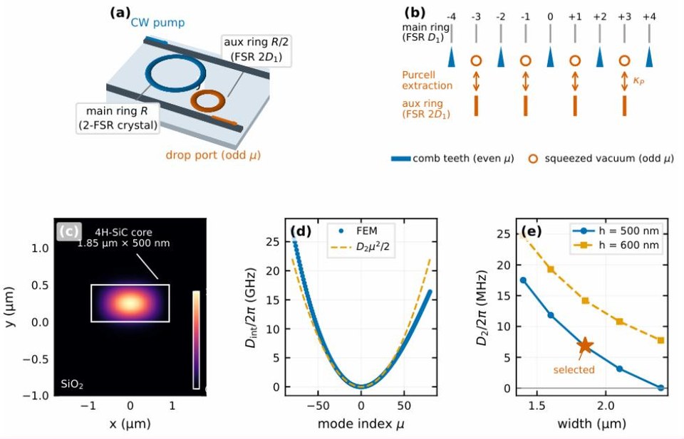
Squeezed light is light whose noise, in the right measurement, falls below the usual quantum limit, a resource for precision measurement and quantum computing. This work builds an open, reproducible pipeline for producing strongly squeezed light in microcombs (micro-rings that turn one pump laser into many evenly spaced colors) on 4H-silicon-carbide-on-insulator. Modeling of the waveguide, simulation of the comb dynamics (Lugiato–Lefever) and a linearized quantum-noise analysis are chained into one workflow, running from material parameters to the noise a detector would record. A single ring faces a built-in trade-off: the coupling that builds up light inside the ring and the coupling that lets the squeezing out oppose each other, so detectable squeezing stalls at 3 dB no matter how hard the ring is pumped. The fix is a second, auxiliary ring, with resonances spaced twice as far apart, which pulls the squeezed modes out while leaving the classical comb untouched. At a fixed 8.3 mW pump, the best extraction rate lies near ten cavity linewidths, and the full two-ring model predicts 7.9 dB of detectable squeezing over 1.81 GHz, rising to 8.5 dB near the boundary of comb stability, and concentrated in two dominant squeezed supermodes with an entangled odd-mode lattice. One more result: third-order dispersion shifts the comb's repetition rate measurably, yet leaves the squeezing unchanged right up to the point where it destroys the soliton crystal. Together with the explicit two-ring design, that answers the two open problems the original photonic-molecule proposal left standing: how much higher-order dispersion the squeezing tolerates, and the design of the molecule itself.
Imaging single vortices in tantalum superconducting circuits
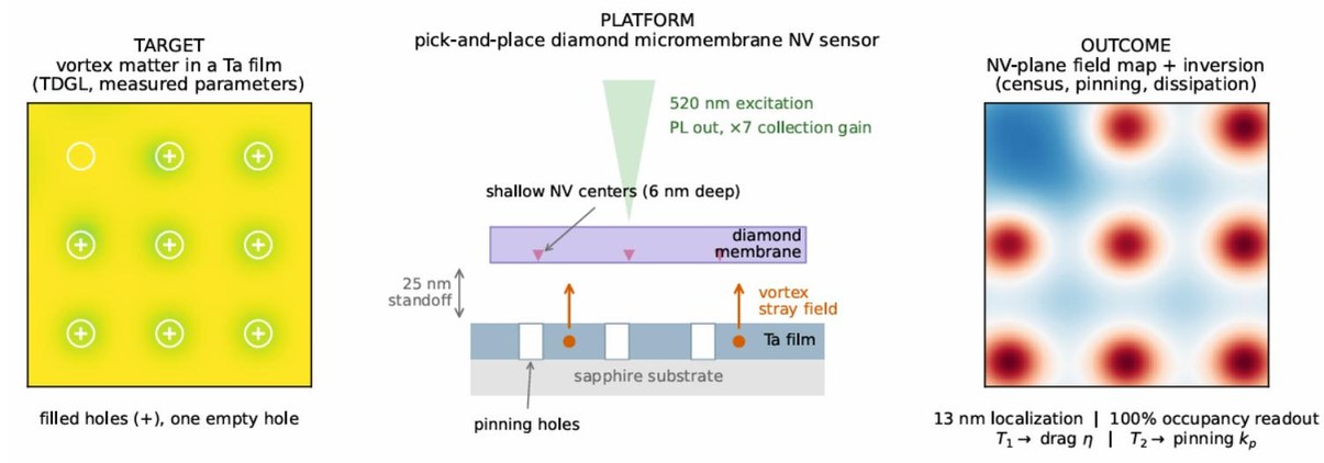
Vortices, tiny whirlpools of magnetic flux, are a confirmed source of energy loss in the clean tantalum films that hold the record for transmon qubit coherence. But no probe available today reports which vortex sits where, how strongly it is pinned, and how much it dissipates. The measurement that identified the loss left two questions open: which density and geometry of pinning sites suffice, and how pinning can be verified hole by hole rather than inferred from an averaged quality factor. This work supplies the missing link. Simulations of vortex behaviour (time-dependent Ginzburg–Landau), anchored to the measured vortex viscosity, generate realistic vortex arrangements. Their stray fields reach 8 mT per vortex at 25 nm standoff, thousands of times above the sensor's noise floor. A physics-based inversion of each vortex's known field shape then localizes every vortex to about 13 nm and classifies pinning-site occupancy without error at 10 µs per pixel, out to a 300 nm standoff. Finally, the sensor's two noise channels separate the two parameters of the loss model: spin relaxation reads how much a vortex drags, and spin-echo dephasing reads how stiffly it is pinned, at a contrast above one thousand; correlating two sensors resolves vortices hopping together.
SPARQ: autonomous triage of solid-state single-photon emitters
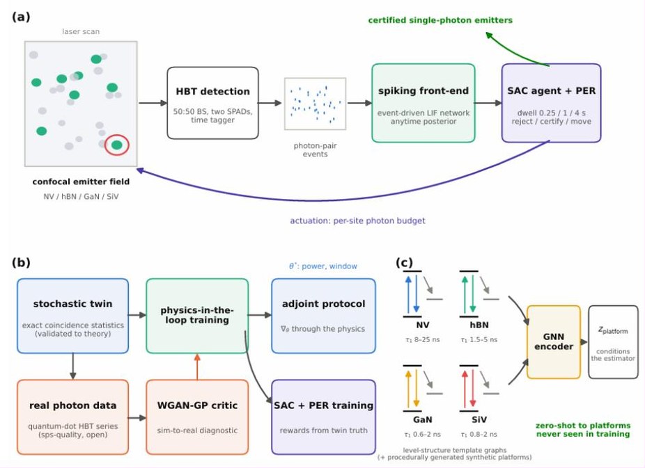
Testing whether a candidate emitter really emits single photons uses the Hanbury Brown–Twiss correlation measurement. At minutes per candidate site, that measurement is the bottleneck of single-photon-source development. SPARQ turns it into a closed-loop instrument that decides as it measures, rather than an offline fitting procedure. At its center is a stochastic, differentiable "twin": a simulator of the measurement chain faithful enough to train against, validated against the numerically exact reference (reduced χ² of 0.86 to 1.21). A spiking neural network trained on the twin's photon-sparse statistics reaches the accuracy of a strong multi-start fit six times faster, committing its median decision 312 ms into the exposure at nanojoule energies. Gradients through the twin also tune the measurement protocol itself, worth 2.7 accuracy points where photons are scarcest. And a reinforcement-learning agent (soft actor–critic) screens fields of emitters 1.7× faster than quality-matched raster scanning.
An oracle bound of 8.8× shows that the physics-trained estimator, not the sophistication of the decision policy, is the decisive lever, worth stating because it directs where effort should go next. On openly published quantum-dot data the twin-trained estimator transfers with no retraining at twice the accuracy of conventional peak-area analysis, within 24% of the information floor, leaving an adversarial refinement stage nothing to add. Encoding each emitter platform's energy-level structure as a small template graph recovers 92% of the remaining transfer gap across nitrogen-vacancy, hexagonal boron nitride, GaN and silicon-vacancy emitters.
PILOT-Q: photon-efficient neural inference at the standard quantum limit
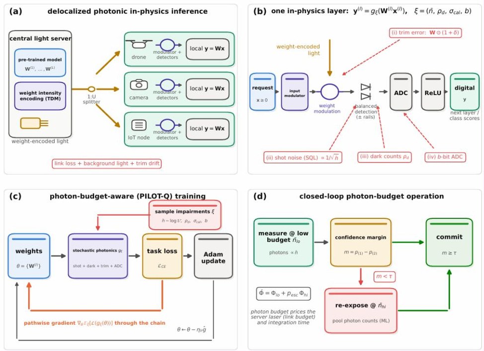
In delocalized photonic inference, a central server broadcasts a neural network's weights as light, and low-power edge devices carry out the arithmetic optically. The useful operating points sit near one photon per multiply, where the arithmetic is governed by shot noise, the irreducible randomness of light detection. Yet such systems are trained assuming clean digital arithmetic, and their photon budget is fixed in advance for the hardest input. PILOT-Q closes both loops. A differentiable stochastic twin of the optical chain (detection with exact shot-noise statistics, dark counts, weight-encoding error and quantization) is validated against the analytic shot-noise law to within 9% over three orders of magnitude in photon budget. Training through it raises photon-starved accuracy from 51.6% to 78.6% at one photon per multiply–accumulate, at no cost when light is plentiful, and cuts the budget needed for matched accuracy by 1.4 to 3.1× on three open benchmarks.
Two results are reported precisely because they are negative. Shot-noise-aware training alone provides the robustness; simulating the full stack of hardware imperfections during training adds nothing and costs peak accuracy. And an oracle analysis bounds even ideal input-by-input adaptivity near 2.0× over conventionally trained static provisioning, because at the quantum limit accuracy rises steeply with photon budget. Training, not run-time adaptivity, is therefore the lever here, the opposite of what noisier analog hardware favors.
FabGAN-ID: learned fabrication twins for yield-aware photonic design
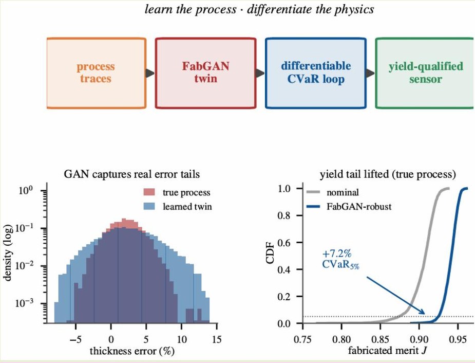
Designs that must survive manufacturing variation are usually optimized against the assumption that the variation is Gaussian (bell-shaped and independent). Real fabrication error is not: it is systematic, correlated and heavy-tailed, and that is what actually governs yield. FabGAN-ID learns the real distribution from the factory's own record, using a generative network (a conditional, moment-matched Wasserstein GAN) trained on only 400 historical process traces. Placed inside a fully differentiable optimization loop with an exact physics solver, the learned model lets the designer optimize the worst-case tail of the yield directly (conditional value-at-risk). That improves the yield floor of a 532 nm fluorescence-rejection notch filter by 7.2% over the nominal design, and outperforms every Gaussian-based robustification method on the true fabrication process. It also supports analytic policy-gradient optimization of specification-conditioned correction policies, where model-free reinforcement learning fails. Released with 48,300 spectra and 400 fabrication traces.
Electrons and phonons in 2D devices
Conducted with Prof. Md. Mosaddequr Rahman, Department of EEE, BRAC University, from July 2024 to July 2026. This work follows charge carriers and lattice vibrations (phonons) through nitride and single-layer semiconductor channels, from the underlying quantum states up to the masses, lifetimes and circuit-level numbers experiments report, and applies physics-in-the-loop inverse design to micromachined transducers.
Resolving the conflicting hole masses of the GaN/AlN two-dimensional hole gas
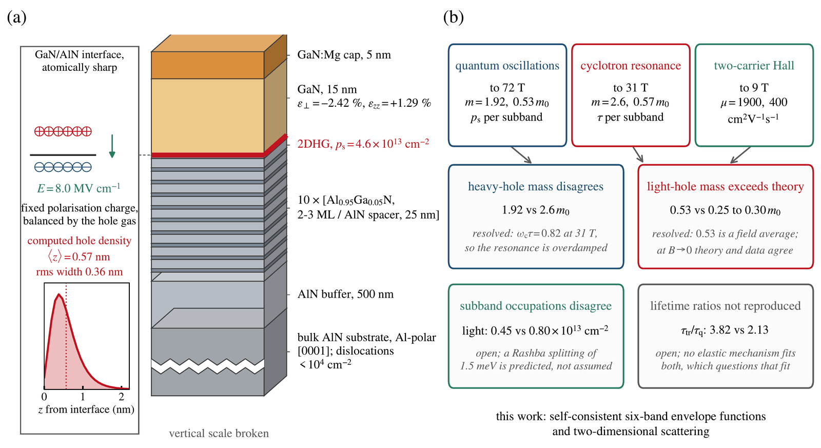
Three careful experiments have all been applied to the same GaN/AlN two-dimensional hole gas: quantum oscillations in pulsed magnetic fields to 72 T, terahertz cyclotron resonance to 31 T, and a two-carrier analysis of the Hall effect. The effective masses they report disagree. This work computes the hole states from the standard six-band quantum model, solved self-consistently with the electrostatics at the measured hole density, with a realistic finite AlN barrier and no adjustable quantity. Any difference in conclusion therefore follows from the analysis, not from the inputs. The calculation reproduces both measured masses. The heavy-hole mass comes out at 1.92 to 1.99 m0 across the published range of the valence band offset, against a measured 1.92 ± 0.16 m0; the zero-field light-hole mass comes out at 0.26 to 0.33 m0, against the 0.30 m0 the measurement extrapolates to at zero field. The band structure is therefore not in question, and the reported light-hole mass of 0.53 m0 turns out to describe how the mass changes with magnetic field, not the band structure itself. Why do the two magneto-optical probes disagree on the heavy mass by a third? Because at the highest field applied, the heavy-hole resonance is overdamped (its cyclotron product ωcτ is 0.82, below the threshold of one for a clean resonance), while the light-hole resonance is clean at 3.8, and the light masses agree to seven percent.
On scattering, one ratio does the work. The ratio of transport to quantum lifetime depends on neither the disorder strength nor the mass, so it isolates one thing: how far the disorder reaches. Its measured value requires long-range disorder that deflects carriers only gently, through small angles, and not the short-range mechanism it has been attributed to. And with the overlap between bands computed from the wavefunctions rather than assumed, no elastic scattering mechanism reproduces the measured ratios of both subbands at once; the closest simultaneous account is wrong by a factor of two. That places the standard two-carrier decomposition of the mobilities itself under question. The predicted density dependence of both masses is stated as a direct experimental test.
Two Raman phonons that measure edge charge in monolayer nanoribbon transistors
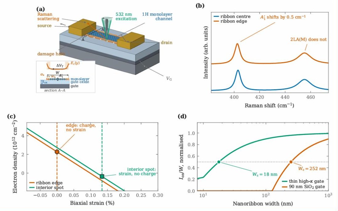
Cutting a monolayer into a ribbon exposes an edge, and that edge carries fixed electric charge and mechanical strain together. Neither has been measured separately at such an edge, because a single Raman frequency responds to both at once. And without a measured edge charge, the minimum useful width of a nanoribbon transistor cannot be predicted. The way out is a pair of frequencies. First-principles (frozen-phonon) calculations on the four 1H monolayers MoS2, WS2, MoSe2 and WSe2 show that the strain response of the disorder-activated 2LA(M) mode is several times that of A′₁, while only A′₁ responds to carrier density. Two frequencies, two causes, cleanly separable. Applied to published tip-enhanced Raman maps of patterned MoS2 nanoribbons, the method returns an edge excess of 2.3 × 10¹² ± 7.6 × 1011 cm-2 of band electrons with strain below 0.03%, and identifies an interior feature in the same map as pure 0.134% tension carrying no charge.
Carried into a self-consistent electrostatic and transport model, charge of that size explains a reported switch in transistor behaviour (from depletion- to enhancement-mode) on thick-oxide devices. Yet the same charge has no electrostatic effect on a thin high-κ gate, where the damage halo left by the etch instead sets the critical width: 18 nm, rather than the 252 nm of the thick-oxide stack. The as-grown defect density, inferred here from published disorder-activated Raman ratios, rescales the current a ribbon delivers but barely moves that width. The result is a non-destructive optical route to the electronic state of a patterned edge, needing only two phonon frequencies a nanoscale Raman probe already resolves.
Strain and ferroelectricity together in WSe2 nonvolatile logic
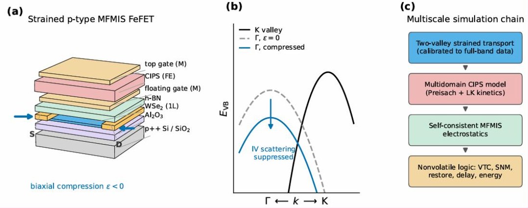
Strain engineering and layered (van der Waals) ferroelectrics have each advanced two-dimensional electronics, but their combination had not been examined. This end-to-end study unites them in a single memory transistor: a monolayer WSe2 channel under process-induced compression, gated through a CuInP2S6 metal–ferroelectric–metal–insulator–semiconductor stack. A two-valley transport model, calibrated against published full-band calculations and strained-transistor measurements, feeds self-consistent electrostatics coupled to a realistic multidomain (Preisach and Landau–Khalatnikov) description of the ferroelectric. The headline: one percent of compression more than doubles the hole mobility, because compression separates the energy valleys between which carriers scatter. The benefit carries over intact to the memory function. Retained on-current rises 1.8×, while the 1.24 V memory window of a 30 nm stack moves by only about three percent, so strain and polarization are independent design variables. At circuit level, the resulting complementary nonvolatile inverters and latches recover their state within 2 ns of complete power loss, cut worst-case static power by eight orders of magnitude against the reported resistor-loaded CIPS latch, and gain 2.3× in energy–delay product.
PARL-ID: fabrication-aware inverse design across MEMS and photonics
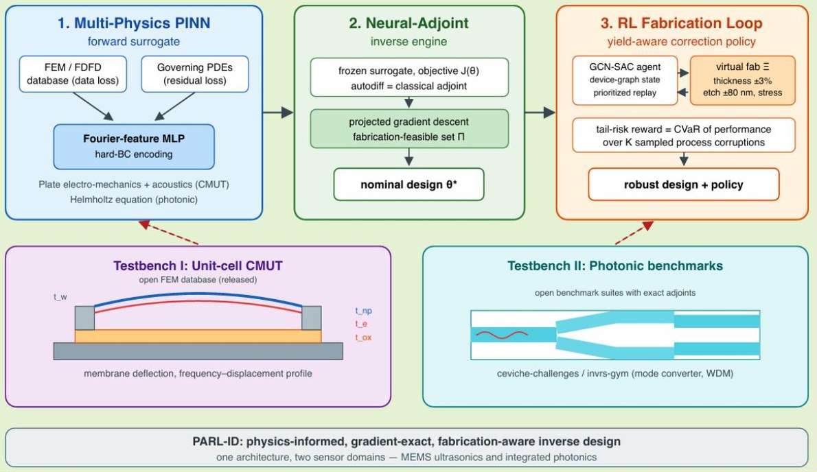
PARL-ID unifies physics-informed neural networks, adjoint (gradient-based) optimization and reinforcement learning into a single framework for designing sensors that stay within specification when manufacturing varies. Validated on micromachined ultrasound transducers (CMUTs) and on photonic benchmarks, it improves optimization efficiency while producing fabrication-tolerant designs that outperform conventional data-driven inverse design. It is the direct successor to the published CMUT framework described below: that work identified the best network architecture for a nominal design; this one optimizes for designs that survive process variation.
Hierarchical inverse design of unit-cell CMUTs
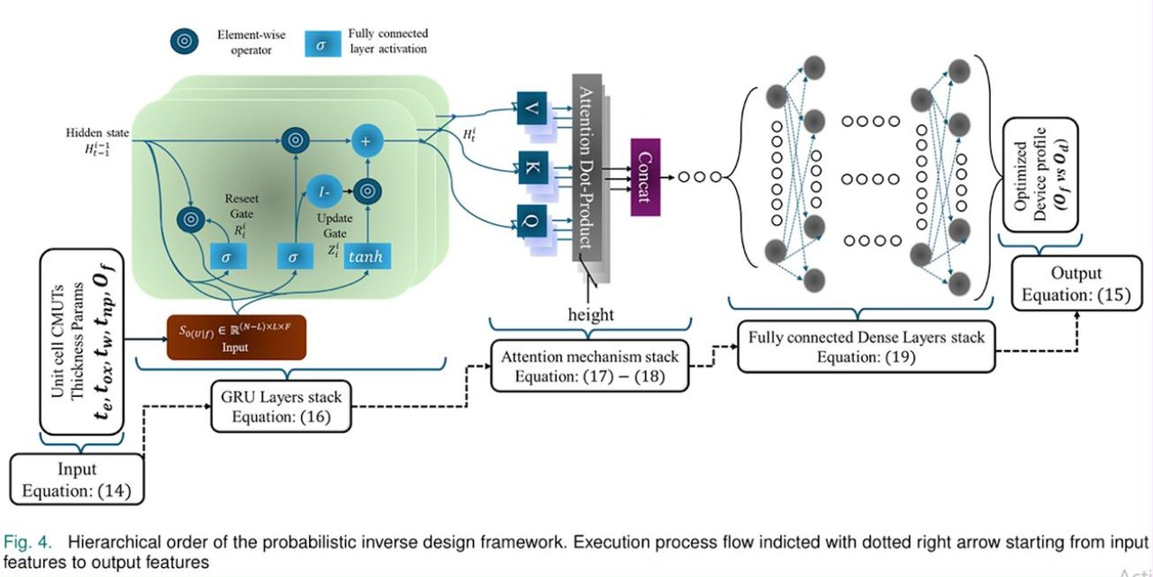
Designing a micromachined ultrasound transducer normally means a manual sweep over device profiles. In this published work, a probabilistic search first identifies the machine-learning architecture best suited to the task (attentive gated recurrent layers feeding fully connected dense layers), and that network then maps a target acoustic response back to unit-cell CMUT geometry, maximizing membrane displacement without the exhaustive finite-element sweeps that unit-cell design normally demands.
Differentiable design of GaN circuits
Conducted with Dr. Nadim Chowdhury, Department of EEE, BUET, from May 2025 to June 2026. This work carries gradients through the compact models and the loop equations of a GaN circuit, so that the circuit can be designed by optimization, and develops reinforcement-learning methods that transfer across process nodes.
Co-designing a monolithic GaN-on-SOI fractional-N PLL
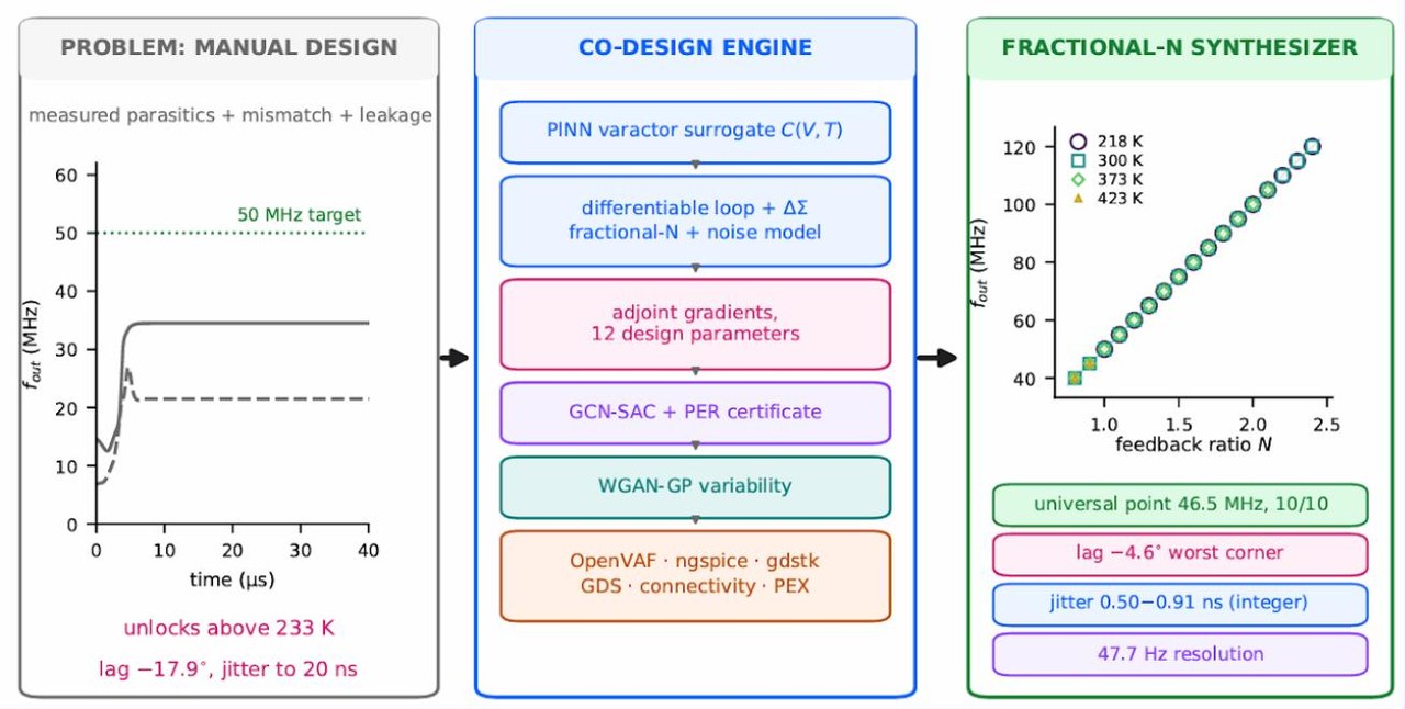
This work automates the co-design of a complete frequency-synthesizer circuit, a monolithic fractional-N phase-locked loop, in 200 V GaN-on-SOI technology. Physics-informed neural networks, adjoint-based gradient optimization and graph-based reinforcement learning jointly optimize circuit performance, thermal robustness and manufacturability: three objectives that are conventionally traded off by hand, one at a time. The resulting PLL shows substantially reduced phase error and jitter, improved lock yield, a compact layout implementation, and reliable fractional-N operation across a wide temperature range.
Transferable analog transistor sizing with graph reinforcement learning
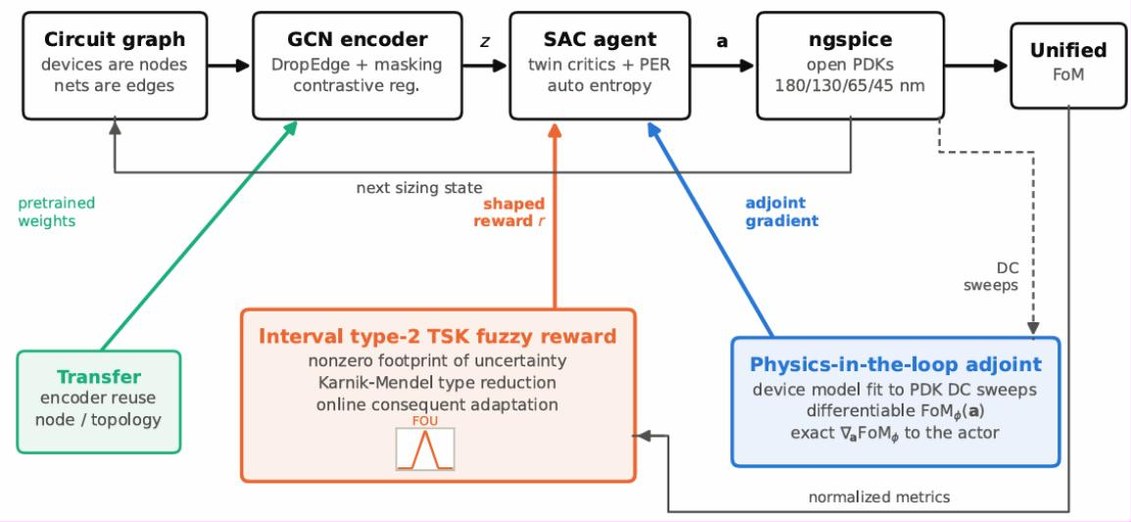
Developed with GlobalFoundries, Inc., this framework sizes analog transistors automatically. A graph network reads the circuit (devices as nodes, wires as edges), a reinforcement-learning agent proposes sizes, a fuzzy reward model carries the uncertainty in what "good" means, and physics-supplied gradients guide the search directly. Whereas conventional approaches rely on black-box circuit simulation and fixed weighted objectives, this combination improves both the quality of the result and the number of simulations needed to reach it. Validated across multiple technology nodes and amplifier benchmarks, it consistently outperforms existing Bayesian-optimization and reinforcement-learning methods while transferring across circuit topologies.
Intelligent grid control
Conducted with Dr. A. H. M. A. Rahim (retired December 2024) from May 2023 to June 2024. This work develops controllers that adapt their own inference rules, applied to grid-connected machines under fault conditions.
Fuzzy inference with reinforcement learning for DFIG low-voltage ride-through
How much wind generation a grid can accept is limited by what happens during faults. This work couples a Takagi–Sugeno–Kang fuzzy inference engine (control rules expressed in graded, human-readable form) to reinforcement learning, so that the controller adapts its own rules rather than relying on a fixed rule base. It sustains a doubly-fed induction generator, the standard wind-turbine generator, through voltage sags severe enough to defeat conventional ride-through schemes.
Adaptive fuzzy attention control of a microgrid under grid-bus fault
A double Q-learning scheme with prioritized rewards drives an attention-weighted fuzzy inference controller, keeping a microgrid stable through an extreme fault on the grid bus. This is the regime in which fixed-gain controllers fail, because the operating point departs further from nominal than their tuning assumes.
Photovoltaic modeling: from cell physics to systems
Conducted with Dr. A. H. M. A. Rahim and Prof. Md. Mosaddequr Rahman between 2023 and 2026. A custom-built bifacial module was characterized experimentally and then modeled from the one-diode equations upward.
Weather-responsive efficiency model for a custom-built bifacial panel
Standard efficiency-rating models account only for sunlight intensity and ambient temperature. Starting from the derivation of the one-diode model toward a photovoltaic efficiency rating, this work introduces air pressure and humidity as additional, carefully constructed dimensions, and validates the resulting model against modules based on several different cell technologies, including a bifacial panel constructed and characterized in-house.
Mono- and bifacial photovoltaic technologies compared
Next-generation bifacial cells (panels that collect light on both faces) are central to the development of high-efficiency modules. This review compares the emerging technologies, including TOPCon and silicon heterojunction, with their monofacial equivalents on a common basis.
Agrivoltaics: challenges and prospects
Agri-photovoltaics enables the dual use of land for agriculture and electricity generation. This review surveys recent agri-PV prospects across continents, together with the standards, community-acceptance and policy questions that determine whether the economic benefit reaches the farmers working beneath the arrays.
Open-source software
Beyond the per-paper repositories above, eight general-purpose tools distilled from this research (ramansep, kpenvelope, sqzcomb, absnoise, cavsqueeze, SPARQ, hamop and fabtwin) are maintained under the TaN-MM-Org organization, with tested cores, continuous integration and archived DOIs. They have a page of their own: Software.